Sony Stacked Sensors are not the Old (2012) BSI Sensors
May 13, 2023 18:58:30 #
larryepage
Loc: North Texas area
Earlier this afternoon, I got in some trouble by stating that the Stacked CMOS Sensors are a completely different animal from the BSI sensors used in the D850 and some other cameras. Specifically, I was informed that the stacked sensors ARE BSI (Back Side Illuminated) sensors and that "it makes me look bad" to claim that they are not.
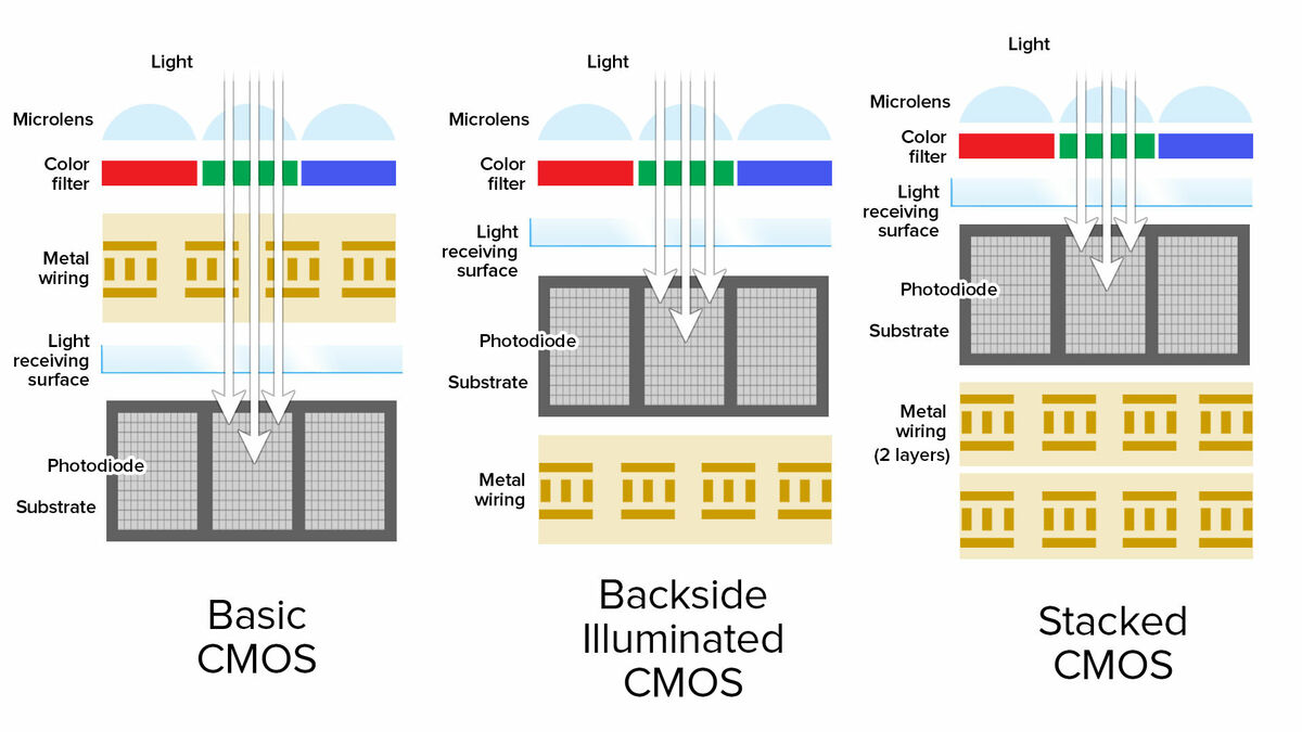
First...BSI sensors are monolithic sensors. While they are made up of two (or perhaps more) layers of components, they are built as single entities. In order to maintain the physical tolerances necessary for proper optical performance, they are built with the sensor elements (photodiodes) on the bottom...against the silicon substrate material. Once the sensor level is complete, an insulating layer is put down, and the semiconductor fabrication process continues, with amplification, logic, and control circuitry built on top of the sensor layer. What comes out of the foundry is a single device, waiting to be wired into a camera. Except for one thing. The silicon substrate on the bottom (back) is opaque, and so is most of the circuitry constructed on the top of the sensor. So an additional step is necessary. The substrate silicon must be mechanically ground away, exposing the photodiodes to light from the bottom (back) of the circuit...hence the name "Back Side Illuminated. These sensors have been around for quite a while...since 2012. They are actually really old in "semiconductor years."
Stacked CMOS Sensors are a whole different animal They are made in pieces. The first, in 2017, emulated the BSI design by building the photodiode & transistor layer on one wafer and the amplification/control/communication/whatever else on a separate wafer carefully designed to exactly fit and connect to the sensor layer. Since chips from these two completely separate wafers had to be carefully aligned connected ("stacked"), a whole new name was invented...Stacked CMOS sensor. But there is nothing remotely "Backside" about it...the build of the sensor layer is now just like the design of any other sensor , and light enters it from...wait for it...THE FRONT. No grinding, no upside down fabrication of components. It's a whole new world.
But this wasn't the end. In 2021, another big advance was made. Instead of stacking two pieces, Sony figured out that if they stacked THREE pieces, the pixel transistors could be moved to their own layer. This means that instead of the photosites occupying about half of the sensor area and the pixel transistors occupying the other half, the photodiodes can now have the entire sensor surface for their home. They can either be made larger, which means that they can be made more sensitive and ISO ranges can be extended even further or that resolution can be drastically increased without having to give up pixel area. WHAT A DEAL!
So...the new sensors in the Z9 and Z8 are not BSI sensors. Nikon does not call them that. They are STACKED Sensors. Not the same. I suspect that they are the older (2017) two-layer sensors, because I doubt there is any way Sony and Nikon could have gotten a three-layer into a Z9 in less than a year.
For those of you who care, I'll come back in a few minutes with more information so that you can read for yourself from both Sony Semiconductor Solutions Group and Nikon.
May 13, 2023 19:00:52 #
larryepage
Loc: North Texas area
larryepage wrote:
Earlier this afternoon, I got in some trouble by s... (show quote)
Here are two links...one to SSSG and one to Nikon. They include pictures. Some of the pictures are in color.
https://www.sony-semicon.com/en/news/2021/2021121601.html
https://www.nikonusa.com/en/nikon-products/product/mirrorless-cameras/z-8.html
Go down and find the button that says "Compare to Z9 and D850. Click on that button.
There's a lot more information available about this. This is all I'm going to dig out for you.
May 13, 2023 20:35:17 #

larryepage wrote:
Right easy to get confused. My Om-1 utilizes a stacked CMOS sensor so I had to know what that was before I bought it. The stacked technology also enables greater data rate transfer from the sensor which translates to improves continuous shooting frame rates.Earlier this afternoon, I got in some trouble by s... (show quote)
May 13, 2023 20:38:34 #
larryepage wrote:
modern digital cameras are amazing systems, they use all the technology available and they might be even more complex than RADAR.Earlier this afternoon, I got in some trouble by s... (show quote)
May 13, 2023 23:26:07 #
May 13, 2023 23:37:37 #

Larry said
"So...the new sensors in the Z9 and Z8 are not BSI sensors"
This is incorrect.
In fact the sensor is "Stacked BSI CMOS" tech
See pages 3-4 here:
https://www.uglyhedgehog.com/t-773782-3.html
---
---
"So...the new sensors in the Z9 and Z8 are not BSI sensors"
This is incorrect.
In fact the sensor is "Stacked BSI CMOS" tech
See pages 3-4 here:
https://www.uglyhedgehog.com/t-773782-3.html
---
---
May 14, 2023 00:45:59 #
Bill_de wrote:
Larry said
"So...the new sensors in the Z9 and Z8 are not BSI sensors"
This is incorrect.
In fact the sensor is "Stacked BSI CMOS" tech
See pages 3-4 here:
https://www.uglyhedgehog.com/t-773782-3.html
---
---
"So...the new sensors in the Z9 and Z8 are not BSI sensors"
This is incorrect.
In fact the sensor is "Stacked BSI CMOS" tech
See pages 3-4 here:
https://www.uglyhedgehog.com/t-773782-3.html
---
---
Correct , the Nikon Z9 and Z8 have the exact same 45mp stacked BSI sensors , as do the Canon R3 (24mp), Sony A9, A9II (24mp) , A1(50mp) , Sony RX10 IV (24mp) also all have stacked BSI CMOS sensors.
Larry couldn't refute all the evidence against his ridiculous "stacked sensors are not BSI sensors" in another long thread on the new Nikon Z8 with its stacked BSI CMOS sensor (the same sensor as in the Nikon Z9) , so Larry created his own new thread here to spread more of his technical inaccuracies and misinformation.
Larry you are still wrong, even if you create your own thread to spread fake information. You cant run and hide from the facts of stacked BSI CMOS sensors, by creating your own separate thread , LOL
Larry thinks sensors have to be either stacked or BSI. Larry tried to sell that falsehood in the Nikon Z8 stacked sensor thread, and nobody was buying that . Larry has no real understanding of the tech and the construction of BSI stacked sensors, even when he sees the illustrations and is presented with the facts.
From DXOMark: " The Sony Alpha 1 is the new Sony full-frame mirrorless flagship, sitting above the Sony A9 and the Sony A7 models. Housed in a familiar-styled and still relatively compact body, the Sony A1 features a completely new 50 MP “stacked” BSI CMOS sensor capable of 30 fps bursts (lossy compressed RAW/JPEG only), blackout free, and captures 8K/30p video."
https://www.dxomark.com/sony-a1-sensor-review-speed-and-quality-in-one/
From PC Magazine: " The A1 sports a brand-new sensor, one that shares the Stacked BSI CMOS tech that allows the a9 to capture photos silently and without any blackout, but with more than twice the resolution—50MP. To deliver a clear view from the sensor, Sony has upped EVF resolution and size (9.4 million dots, 0.9x magnification) and improved its refresh rate to 240fps."
https://www.pcmag.com/news/sony-a1-marries-stacked-sensor-tech-with-50mp-capture
From DPReview and Tech Insights: "The Sony IMX610AQL is a full frame (FX format), 50.1 MP, 4.16 μm pixel pitch, stacked back-illuminated (ExmorRS) CMOS image sensor from the Sony Alpha 1 (ILCE-1) MILC."
https://www.dpreview.com/news/2070774702/sony-s-flagship-a1-camera-appears-to-be-using-an-exclusive-imx610-image-sensor#:~:text=Sony's%20flagship%20a1%20camera%20appears%20to%20b
The illustration below of Sony's (ExmorRS) 50mp Stacked BSI sensor in the Sony A1 is from Sony's own website.
From Imaging Resources: " The Sony A1 has the highest megapixel count of the three. It beats out the 45.7MP Nikon Z9 by a small margin. However, the Canon EOS R3 lags at 24.1MP. All three cameras incorporate a stacked, backside-illuminated CMOS image sensor."
From B&H Photo and Nikon in their intro to the Z9: "The core of the Z9 is the newly developed FX-format 45.7MP BSI stacked CMOS sensor. Its stacked design offers fast readout speeds and helps to reduce rolling shutter, and the BSI design contributes to impressive clarity and minimal noise when working at higher sensitivities."
From Canon-Europe: "Mastering movement at 30fps. At the heart of the EOS R3 is a backside-illuminated, stacked sensor – developed exclusively by Canon. It is faster and more sensitive than anything we've put in a camera before, which means better performance when you're shooting under pressure."
As EVERYONE else in the photo world but Larry knows, these sensors are BOTH BSI and stacked. Looks like nothing will get through to him, not even from Nikon, Sony, Canon or from any top photo tech experts and testing groups, so sad. Larry is a lost cause here for sure on this. Best to just ignore Larry here on this subject and move on. He seems oblivious to the truth.
Of course the newer stacked BSI CMOS sensors in more recent cameras like Sony A9 (released 2017) , A9II (released 2019) , A1 (released Jan. 2021), Canon R3 (released Nov. 2021), Nikon Z9 (released Dec. 2021), Z8 (released May 2023) , Sony RX10IV (released Sept. 2017) are NOT the old and non-stacked BSI sensors of 2012, but they are stacked BSI CMOS sensors of recent years and today.
Larry refuses to admit the reality of that truth.
You can lead a horse to water, but can't make it drink, seems appropriate here for Larry , sadly.
Cheers and best to you all.
May 14, 2023 03:10:03 #

The only product that uses the new stacked photodiode construction is the Experia 1 V smartphone. It hasn't found its way into camera sensors yet.
Up to now, "stacked" meant faster and less noisy readouts. Stacking the photodiodes has a far bigger effect on image quality because it increases the sensor's light-capturing capability. It also allows the use of larger, less noisy transistors, which is an added benefit. Photodiode stacking is more significant for smaller sensors than larger sensors, but overall it's a significant step forward in sensor design.
Up to now, "stacked" meant faster and less noisy readouts. Stacking the photodiodes has a far bigger effect on image quality because it increases the sensor's light-capturing capability. It also allows the use of larger, less noisy transistors, which is an added benefit. Photodiode stacking is more significant for smaller sensors than larger sensors, but overall it's a significant step forward in sensor design.
May 14, 2023 04:55:40 #
Who do you trust? Folks know-it-all on UHH or the manufacturer? (Nikon)
Funny how Nikon differentiates the sensors... Just saying, unless they are mistaken and are not listening to UHH 'experts'.
Funny how Nikon differentiates the sensors... Just saying, unless they are mistaken and are not listening to UHH 'experts'.
May 14, 2023 05:10:20 #
This time Sony website source...
Pray tell, where are the backlit elements in their new sensor?
Oh, right, Sony does not know what they are doing but UHH folks do.

Pray tell, where are the backlit elements in their new sensor?
Oh, right, Sony does not know what they are doing but UHH folks do.
May 14, 2023 10:37:45 #
larryepage
Loc: North Texas area
Rongnongno wrote:
This time Sony website source...
Pray tell, where are the backlit elements in their new sensor?
Oh, right, Sony does not know what they are doing but UHH folks...
Pray tell, where are the backlit elements in their new sensor?
Oh, right, Sony does not know what they are doing but UHH folks...
These illustrations that you have posted are from the two PRIMARY references that I listed. They clearly support what I have said. I do not care nor pay attention to what some nitwit has claimed in any SECONDARY reference.
This has been a quite illuminating discussion and speaks volumes about the validity and reliability of the information available here. The full extent of misinformation is shocking.
May 14, 2023 11:20:29 #
Rongnongno wrote:
Rongo, A back-illuminated sensor, also known as backside illumination sensor, is a type of digital image sensor that uses a novel arrangement of the imaging elements to increase the amount of light captured and thereby improve low-light performance.This time Sony website source...
Pray tell, where are the backlit elements in their new sensor?
Oh, right, Sony does not know what they are doing but UHH folks do.
Pray tell, where are the backlit elements in their new sensor?
Oh, right, Sony does not know what they are doing but UHH folks do.
May 14, 2023 11:20:53 #
May 14, 2023 11:36:18 #
larryepage
Loc: North Texas area
JD750 wrote:
Rongo, A back-illuminated sensor, also known as backside illumination sensor, is a type of digital image sensor that uses a novel arrangement of the imaging elements to increase the amount of light captured and thereby improve low-light performance.
That's what I thought. Like pre-exposing film to get past the knee of the response curve in the old days. But it's not that at all. More misinformation.
BSI is a manufacturing "trick" to building a sensor by putting the sensor elements on the bottom, then grinding the substrate (the base) off so light can get in. It's a pretty inconvenient way to make a sensor, actually, and there was pretty strong motivation to find a way not to have to do it any more.
You can actually read about those on the SSSI website also. It will be interesting to see if the BSI sensors get replaced in the cameras that have them now that there's no longer a reason to go through the pain and suffering to make them.
May 14, 2023 11:37:42 #
When Nikon, Canon, Sony, DXOMark, DPReview, Image Resources, Tech Insights and all others tell you that the Canon R3, Nikon Z9 and Z8, Sony A9, A9II, A1, RX10IV ALL have stacked BSI Sensors, are you going to believe them or believe Larry, LOL
Use your common sense here or drink Larry's Kool-Aid, LOL
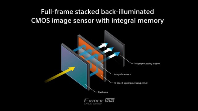
Photo 1: Sony's ExmorRS 50mp fullframe stacked BSI sensor in the A1. Illustration from Sony
Photo 2: Diagram that shows the Stacked sensors are the same technology as BSI, but with added layers. Larry just cant seem to understand this fact that modern stacked sensors are ALSO BSI sensors with added layers.
"Stacked BSI CMOS sensors take the BSI CMOS concept to a further step. They place components in a similar backside illuminated arrangement, but the design also stacks the image signal processor and its ultra-fast DRAM memory into the same silicon. This makes readout speeds even faster."
THIS IS WHAT LARRY CANT SEEM TO GRASP, lol
Cheers and best to you all.
Use your common sense here or drink Larry's Kool-Aid, LOL
Photo 1: Sony's ExmorRS 50mp fullframe stacked BSI sensor in the A1. Illustration from Sony
Photo 2: Diagram that shows the Stacked sensors are the same technology as BSI, but with added layers. Larry just cant seem to understand this fact that modern stacked sensors are ALSO BSI sensors with added layers.
"Stacked BSI CMOS sensors take the BSI CMOS concept to a further step. They place components in a similar backside illuminated arrangement, but the design also stacks the image signal processor and its ultra-fast DRAM memory into the same silicon. This makes readout speeds even faster."
THIS IS WHAT LARRY CANT SEEM TO GRASP, lol
Cheers and best to you all.

If you want to reply, then register here. Registration is free and your account is created instantly, so you can post right away.