Posts for: mawyatt
Jan 9, 2018 14:06:58 #
If you decide the strobe route, the Adorama (Godox SK300II) Studio 300 AC & R2 Remote have worked well for me, same for others over at: http://www.photomacrography.net
The image on the site opening was shot with these strobes & R2 Remote. I routinely shoot multiple sessions of 300~600 stacks and they don't give me any overheating, misfires, missed frames nor inconsistent output problems.
The image on the site opening was shot with these strobes & R2 Remote. I routinely shoot multiple sessions of 300~600 stacks and they don't give me any overheating, misfires, missed frames nor inconsistent output problems.
Dec 30, 2017 00:29:20 #
Here's another version of the circuit. This was shot with D850 EFCS and continuous lighting from 5 studio strobes modeling lights and 4 Ikea LEDs lights. Processed with Zerene Pmax & Dmax.
Best,
Mike
Best,
Mike

Dec 29, 2017 15:12:35 #
mawyatt wrote:
Hi Dave, br br Yes Indium Phosphide (InP) does su... (show quote)
Edit: added "smaller than". Sorry for my misleading omission.
Check out Astronomical Photography Forum section of our forum.
Dec 29, 2017 10:48:52 #
Uuglypher wrote:
Hi, mawyatt, br I never fail to marvel at the scal... (show quote)
Hi Dave,
Yes Indium Phosphide (InP) does suffer from similar process variations as Silicon, and selective doping is used to create the different desirable electrical properties. InP is the base semiconductor like Silicon, and is processed similarly. It is used because of specific electrical properties (charge mobility, bandgap) that allows operation at higher frequencies than traditional Silicon.
Silicon CMOS is the most advanced semiconductor technology in general, with chips being just shipped at 10 nanometer feature size. To put this in perspective a Silicon atom is about 0.2 nanometers wide and the wavelength in free space of green light is ~550 nanometers. So these 10nm process Silicon chips are working fundamentally at a minimum of ~20 atoms and 55 times the wavelength of visible photons!! Truly incredible!
Best,
Mike
Dec 29, 2017 09:22:59 #
Tikva,
Thanks. The density of todays silicon CMOS is such that an entire intel 386 processor can be placed under a typical bond pad (~100 microns square)! These CMOS processes routinely produce chips with well over a billion devices!
Best & Happy Holidays,
Mike
Thanks. The density of todays silicon CMOS is such that an entire intel 386 processor can be placed under a typical bond pad (~100 microns square)! These CMOS processes routinely produce chips with well over a billion devices!
Best & Happy Holidays,
Mike
Dec 26, 2017 17:49:45 #
Thanks MJL. Well it is kind of an entry for electrons :>)
Best & Happy Holidays, Mike
Best & Happy Holidays, Mike
Dec 26, 2017 14:45:47 #
Thanks all. Yes Mark it's more difficult, vibration becomes a major obstacle to achieving acceptable results and sources must be rooted out and eliminated or reduced significantly.
Check out Underwater Photography Forum section of our forum.
Dec 26, 2017 11:40:37 #
GalaxyCat wrote:
Yes in Indium Phosphide, not Silicon. Detect RF and Microwave energy. Test chip. Yes, I design chips among other efforts. Here's the ugly black area edited out.So this is an integrated circuit? What is its purpose? Why isn't it in a package? yet? Is this part of your job?

Dec 26, 2017 09:11:50 #
Here's a tiny InP Test Chip. This image was created with the Mitutoyo 20X and Sigma 200mm LSA as a tube lens. Stack was about 330 images at 2.5 microns.
I had to file the head down of the smallest pin (0.5mm dia) to mount the chip.
In the image note the brown large squares, these are through vias to the chip backside, also the probe scribe marks on the end pads. Another consumption of my time, besides posting here, is indicated in the ULC.
Best & Happy Holidays, Mike


Nov 28, 2017 11:13:18 #
Bozsik wrote:
Jumpers, among other inverts. It happens in a blink of an eye. Nature made.
I think it turned out ok.
I think it turned out ok.
That's awesome!! Did you use the SB800 speed light?
Best,
Mike
Nov 27, 2017 08:21:54 #
Chris,
A Photon :>)
Best,
Mike
A Photon :>)
Best,
Mike
Check out AI Artistry and Creation section of our forum.
Nov 26, 2017 16:07:44 #
Mark, Here's a couple images of an old 6" silicon wafer with the Nikkor PN105 and PN105 with the Nikon TC 1.4 III using the mentioned modded F mount adapter.
https://nis.nikonimagespace.com/html/guest/detail.html?g=5xCFhBeto_SZNLlFwfJrtq8BMuZ1cHP-VOWqtI1SvWrRz7FEIqwgOyJ9zuSZkZMV5GDJJmfsIdM4z6sAtrPhKZqw3G-FHVJCabIh2gb7LztLYhIr9fox_6mqBbSgPe3iA5XIoBLwptE
https://nis.nikonimagespace.com/html/guest/detail.html?g=5xCFhBeto_SZNLlFwfJrtq8BMuZ1cHP-VOWqtI1SvWrRz7FEIqwgOyJ9zuSZkZMV5GDJJmfsIdM4z6sAtrPhKZqw3G-FHVJCabIh2gb7LztLYhIr9fox_6mqBbSgPe3iA5XIoBLwptE
Nov 19, 2017 14:08:52 #
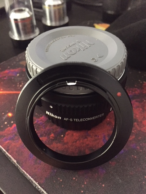
Wanting to use my Nikon TC-1.4E III teleconverter has been limited to those lens from Nikon that were "compatible". Some folks have modified the TC to allow use with other lenses and such, but I was not just yet ready to grind off the TC flange tap on this expensive TC that prevents use on "non-compatible" lens.
Recently someone (Lou over on Photomicrography) has done some tests with the Printing Nikkor PN105mm F2.8 which is a highly optimized lens at 1X, and used the modified Nikon 1.4TC to extend the PN105 to 1.4X while keeping the PN105 at it's design center of 1X. The PN105mm is considered one of the sharpness lenses at 1X, with edge performance equal to center, see Coinimaging.com.
Well I haven't got to where I am comfortable grinding off the tap on the TC, so I thought about modifying a cheap eBay Nikon F mount adapter to work with the TC since this allows use with extension tubes, adapters and such.
I used my Nikon AFS 80-400mm and Nikon 1.4TC mentioned as guides on what needed to be done to allow the F fount to fit to the TC. Many of Nikon lenses will not work with this TC, but many longer modern Nikon lens are compatible, like the AFS 80-400.
Note the 3 locking flange taps sections in the lens mount, these are located about 120 degrees apart. Also note that the tap near the White lens alignment dot, to the left is split into 2 taps, one is short about 4.4mm with only ~3.7mm separating from the longer length tap. This is where the F mount fits into the TC slot which is 5.2mm wide and without this slot in the lens flange the TC won't allow the lens to mate properly.
With the F mount adapter in hand locate the alignment dot (red in my case) and position it above your compatible lens so you can see where the slot must be cut. Before you mark the slot with a pencil on the adapter align the 2 other taps with the lens taps, in my case this is not having the F mount Red alignment dot aligned with the lens White alignment dot, they differ by quite a few mm!! Once you have the flange taps carefully lined up mark the slot on the adapter flange.
I used a Dremel like tool with diamond bits to carefully grind off this slot as shown. It mounted onto the TC the first time and even "felt" like a proper fit.
Now I just need to flock the rear of the adapter and I can use my 1.4TC
Nov 15, 2017 11:23:50 #
Paul,
Yes, that's the technique in Zerene. Here's thread that show the Cross-Eyed version with Zerene. I'm new to all this animation, stereo and cross-eyed stuff, so this was my 1st attempt at any of this (follow thru towards the end for the actual images, but good reading from the start also).
https://www.photomacrography.net/forum/viewtopic.php?t=35798&postdays=0&postorder=asc&start=0
It took awhile for me to actually see the Cross-Eye image, but when I did finally get it...wow!! It looks like a floating hologram to me. I had to fill most of my 27" screen with the dual image and sit back about 3 feet. Be patient and relax your eyes will naturally create the 3rd image in the middle. There's a site mentioned that gives a good explanation and demo of this technique, this helps get things started.
Agree a stable base is important. The Wemacro Vertical Stand is a very well designed stand. It includes the stand, ARCA clamp and X&Y positioning stage with subject mount, for $100 it's quite a good deal IMO. Also used the Wemacro focus rail controller & 4X 0.1NA lens, along with the Adorama Studio 300 Monolight strobes (which are only $100 for Black Friday sale) for lighting. These are superb strobes for macro use since they include a radio receiver, proportional modeling lamp and have a tight uniformity spec. A little shipping foam acts as a good strobe diffuser and I used a styro-foam cup around the subject.
Hope this helps,
Best,
Mike
Nov 15, 2017 08:35:15 #
Paul,
This GIF animated image was produced with a 157 image stack using a focus rail, so only one original image stacking session was involved producing 157 images. The different angles required for animation were created from this original session without physically having to do another session with the focus rail, they were created by a mathematical manipulation of the original 157 images software stacked (Zerene) with different angles of view. So basically 9 software (Zerene) stacking sessions were run on the original 157 images, one for each angle of -4,-3,-2,-1,0 1, 2, 3 & 4 degrees, which created 9 separate stacked images. These 9 stacked images were individually processed with LR and PS, then imported into PS Timeline to render the final GIF animated image.
Hope this helps,
Best,
Mike
Check out Software and Computer Support for Photographers section of our forum.