Using .TIF files vs JPG files in focus stacking, A comparison
Jan 10, 2016 00:14:39 #

naturepics43 wrote:
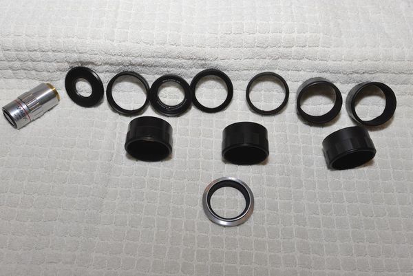
Yes it is a reversed Raynox tube based with a Mitutoyo objective lens. I originally used a lens assembly like some others had done based upon a 42mm extensions, but was getting some vignetting in the corners on a FX (D800) sensor. I found some 52mm extensions used by the astronomy folks and built another reversed Raynox tube based lens around this. Each section and the adapters were all internally flocked with Protostar, which is the blackest material I have even seen, it looks like an optical black hole from any angle!! These custom lenses are shown below.So that's not a reversed Raynox on your tube lens? You mention a special 52mm? Trade secret? LOL!


Jan 10, 2016 00:34:44 #
LoneRangeFinder wrote:
No wood, but I use plastic, although wood is certainly a good dampening material. The big blue plastic tubs are for this exact purpose, high frequency dampening. They support the heavy 1/2" aluminum 1' by 4' base and also produce a slight 20 degree downward tilt. The tilt is to load the focus rail bearings and motor with the help of gravity. I always stack downward so the focus motor doesn't have to work as hard. The plastic tubs and heavy base create what we electrical engineers call a low-pass filter. High vibration frequencies are attenuated by the plastic dampening & base weight. Very low vibration frequencies pass thru but the optical mounting fixture is stiff which causes the subject and camera/lens to move together somewhat. This we call common mode action, while higher vibration frequencies would have the subject and camera/lens not moving together because of the vibration traveling time delay (phase shift) between the subject and camera/lens, we call this differential mode action. The differential mode (due to high frequency vibration) is attenuated by the low pass filter effect of the tub & base.Mike--well obviously you've put a lot of thought and effort into your set-up. I'm curious if you use wood as a dampening material for vibration.
Anyway, this is all theory based, but the results have been better utilizing these concepts than not.....and they didn't cost much at all. Of course I do everything I can to minimize any vibrations in the first place. :)
BTW our very expensive probe stations at work have an air bag supporting a very heavy base which all the exotic probing fixtures mount directly too. This is the same vibration attenuating concept I described above.
Jan 10, 2016 00:47:09 #
rmpsrpms wrote:
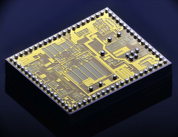
Yes, good spot!! The image with the spiral inductors is part of a very complex Ad-Hoc Networking microwave transceiver SoC. The original SoC design dates back to 2003, an earlier version in 2000 was the most complex mixed signal ASIC IBM had ever done (quote from their CTO & a VP in EETimes), it's also in the book Silicon Germanium BiCMOS Technology dated around that time. We did the design and they fabricated it in an early version of 180nm Silicon Germanium BiCMOS called IBM7hp. Here's some other chips (low res) in this or similar SiGe BiCMOS technologies (ones I can show).Looks like a mmW SOC.
BTW the science behind the solder balls is fascinating, they are called C4 balls. IBM developed this technology many years ago and many years went into it's development, from the chemistry, to the bond formation, surface tension when melted, reflow characteristics and so on. Very complex chemistry & physics went into this seeming simple tiny solder ball!!
Microwave Synthesizer, Note Oxidized Flattened Solder Balls
(Download)
Microwave Transceiver with Damaged & Oxidized Solder Balls
(Download)
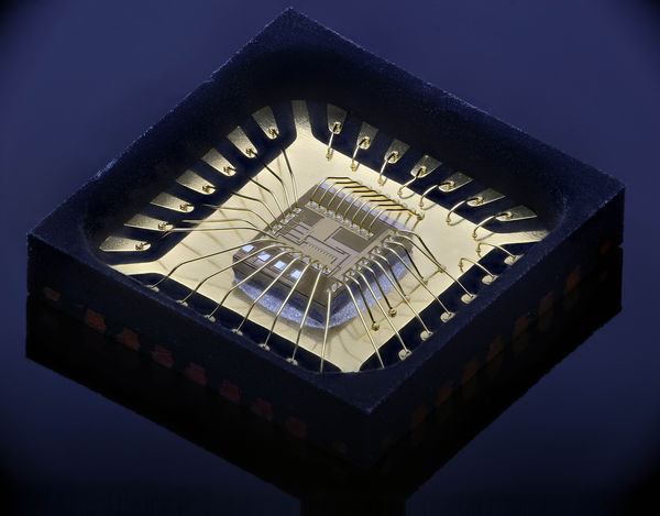
Microwave Digital to Analog Converter, Wirebonded QFN package
(Download)
Jan 10, 2016 10:33:29 #

100um solder balls, very cool. We're using 200um balls on 400um pitch in our MEMS WLCSP packages that solder directly onto the cellphone OEM PCBs. Eventually we'll go with 100um when the MEMS need to be placed inside modules rather than at phone board level.
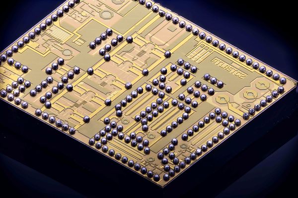
2nd to last image has some nice engineering humor. I can imagine the program name was ATLAS, and the designer gave it the sub-code of TC2, so when put together you get "at last c2". They just forgot the exclamation point!
2nd to last image has some nice engineering humor. I can imagine the program name was ATLAS, and the designer gave it the sub-code of TC2, so when put together you get "at last c2". They just forgot the exclamation point!
Jan 10, 2016 10:56:55 #
One way to understand how this vibration scheme works is to consider this simple thought experiment, you could actually build it if you wanted but not necessary to understand the principles involved.
Take a 4' long beam of something very stiff, say aluminum or steel. Mount your camera & lens on one end and your subject on the other. Focus on the subject then look at the live view at very high magnification. Now slowly lift one end of the beam and move it very slowly (low frequency vibration) up and down. You shouldn't see the image being perturbed because the camera/lens and subject are moving in unison (common mode) to the induced low frequency "vibration". Now "ping" the beam at the end you lifted and moved with a hammer (impulse that contains high frequency vibration) and you should see the image being perturbed (actually this is the mechanical network impulse response (transfer function) for you scientist/engineers/mathematicians). This seems obvious because we all know this is going to "ring" mechanically with the hammer "ping" which acts in differential mode because the camera/lens & subject don't move exactly in unison (they have different phased ringing due to the mechanical time delay between the camera/lens and subject).
At the beam end attach a heavy rubber band and hold the beam by the rubber band and move it slowly up and down, you should see no image perturbation. Now ping the rubber band (or just slightly snap it) on the end you are holding. You should also see no image perturbation.
Well of course not!! We all know why, the rubber band can't transfer the ping to the beam but can transfer the slow movement. This is a low pass mechanical filter, as it passes the low frequencies but not the high frequencies.
In my setup the beam is a heavy aluminum base 1' by 4' & 1/2" thick and the rubber band is the blue plastic tubs. This "network" acts as a low pass filter and the stiffness of the base and attachments helps put low frequency vibrations in a differential mode. The whole purpose is to reduce the image degradation due to external vibrations. Of course you can approach this from any different views.
Wood is another good material for helping reduce vibration influence if used in the right places. Like the rubber band and the plastic tub high frequency vibrations are attenuated, this happens because the rubber, plastic and wood absorb some of the vibration and convert it the form of heat, and also reflect some of the vibration. Wood is stiffer than rubber or some plastics, so the transition where this happens will be at higher frequencies. If you replaced the rubber band with a wooden stick in the above experiment you would think that some of the "ping" vibration might be seen on the image. This is because the frequency where the attenuation begins (called corner frequency) is higher with the wooden stick. Now if you made the mass of the beam 25 times larger, you wouldn't expect to see the ping effects. Why, because you just lowered corner frequency with the heaver beam.
Anyway, hope this helps folks understand the ideas behind my setup and maybe they can apply to their needs.
Jan 10, 2016 11:11:53 #
rmpsrpms wrote:
The program name wasn't Atlas, that was the name of the test chip, and the TC2 is just a reference "Test Chip 2". There has been some engineering humor involved in some chips, but I can't show them. These chips typically have about 4~8 designers involved, although we have employed well over 10 (massive 1 Billion device chip in 28nm that achieves almost 2 tera-operations per second!)100um solder balls, very cool. We're using 200um balls on 400um pitch in our MEMS WLCSP packages that solder directly onto the cellphone OEM PCBs. Eventually we'll go with 100um when the MEMS need to be placed inside modules rather than at phone board level.
2nd to last image has some nice engineering humor. I can imagine the program name was ATLAS, and the designer gave it the sub-code of TC2, so when put together you get "at last c2". They just forgot the exclamation point!
2nd to last image has some nice engineering humor. I can imagine the program name was ATLAS, and the designer gave it the sub-code of TC2, so when put together you get "at last c2". They just forgot the exclamation point!
The smaller solder balls get exponentially more difficult to get right, the 40um balls are really difficult to deal with. We did some of the first flip-chip RFICs back in 95 and also used silicon substrates for larger SoC type die. The idea was silicon flipped on silicon for thermal TC matching. These were with thinned die about 100~150 microns thick.
If you want to reply, then register here. Registration is free and your account is created instantly, so you can post right away.