Posts for: JimH123
Nov 14, 2023 22:43:14 #
gwilliams6 wrote:
IMHO, I think the Canon R1 may well be a global sh... (show quote)
What we don't know is how far along Canon is with their Global Shutter sensor. If they are still experiencing poor noise and dynamic range, would they still release it at that time? Sony had to make a decision on just when it was good enough to release. Is Canon at that point too? We don't know.
I think we can also agree that getting global shutter to actually capture an image is likely the easy part. Getting the IQ they want is the hard part.
Nov 13, 2023 10:55:54 #
mikenolan wrote:
Our 16 year old granddaughter has requested some kind of digital camera for Christmas, she wants one that is lightweight but still has ISO/aperture/shutter speed controls. It should accept filters but does not necessarily need to support interchangeable lenses, but a step up from iPhone or point-and-shoot cameras. (I think lightweight is a key consideration.)
One that she suggested is the NEZINI 4K digital camera, not a brand I am familiar with.
Any suggestions?
One that she suggested is the NEZINI 4K digital camera, not a brand I am familiar with.
Any suggestions?
For a teenager to use a camera, it needs to be small and easy to carry. I bought a used Sony RX100VII and when I want to go somewhere without lugging along a bigger camera, I pick this camera. It can fit in my pocket. I do have the adapter needed to use filters. The early models, I & II, provided a 28-100mm equivalent range at f1.8-4.9. Recent models III & IV provided 24-100mm at f2.8-4.5. The model V was 24-70mm at f1.8-2.8. And models VI & VII are 24-200mm at f2.8-4.5. All models can still be found.
The take superb photos and can be carried inconspicuously. They wouldn't embarrass a teenager.
https://photographylife.com/sony-rx100-series-comparison
Nov 10, 2023 10:49:54 #
larryepage wrote:
It depends. I've taken thousands of images using ... (show quote)
Just google "rolling shutter" and you will see plenty of examples. A plane propeller is the most common example used. Also, when panning a shot to match the speed of something, tall buildings or telephone polls end up leaning. Or even handholding a shot with a telephoto where the camera isn't held steady enough and you are not aimed exactly at the same spot by the time the camera scans the sensor which for many cameras is about 150ms, (that's 0.15 sec!), and it didn't matter that you were using a high shutter speed. Rolling shutter is not uncommon and its a pain.
And mirror slap is indeed a problem with the vibration it causes. It is not hard to see this problem, especially with telephoto or with macro shots.
But if you only shoot using wide to normal lenses and don't shoot fast moving objects or do any panning, then you probably would never see it.
Nov 10, 2023 01:03:44 #
Even the 300mm f/2.8 lens is special. About 3.2 lb. When I use my 300mm f/2.8 lens, it is close to 5 lb. And I think I ought to mount it on the front of a fork lift!
Anyway, fun to drool at what the camera can do. But this old, retired engineer at 73 years old has no hope and no justifiable need for a camera like that. I can still photograph hummingbirds - if they stop flapping their wings that is.
But there are many out there that this is the tool they have been waiting for. And this is just the start. Don't know how long before Sony allows other manufacturers to have access to anything like this sensor. And I expect it won't be exactly this sensor that someone will eventually be able to buy. There will likely be a number of options buyers will have to weigh to figure out what they can afford vs the max Sony can build. Security cameras can probably be built with standard sensor stock that Sony can put a part number on, but most cameras will likely be after something more custom rather than something stock. And that is probably not difficult for Sony to do. I'm sure they have very good layout tools that with someone who knows what they are doing, they can create something more custom in short order.
I know Nikon uses their own sensor designers to create custom sensors for Sony to make. But there are new things here that Nikon is going to have to pay Sony in order to put into their design. Just don't know how long Sony will keep saying "Not Yet!".
Nov 9, 2023 20:19:38 #
gwilliams6 wrote:
PetaPixel's Chris and Jordan: Sony a9 III Initial Review: This Changes EVERYTHING!
https://www.youtube.com/watch?v=pNGLhTDYpYM
https://www.youtube.com/watch?v=pNGLhTDYpYM
Nice entry to the camera. But just as I thought. They are only able to do JPEGs. No access to RAW files. The JPEGs don't show any noise or dynamic range problems. But the RAWs are needed to figure out just how good or bad it really is. We will have to wait for production models for those measurements.
For those that know why the RAWs are needed is that JPEGs are subject to in-camera noise reduction and other processing in the camera hiding what the true image started with. RAWs do not get that in-camera processing and can be used to see how this compares with other cameras.
Results should be interesting as it gives us a pretty good idea of how good a job Sony has done on the first release of Global Shutter.
By the time a global shutter is to go into an A1 series or an A7R series, it needs to be really, really good, in addition to being a whole lot more dense, with a lot more data processing.
Also, that brings up the question on just when Sony will start selling these kinds of sensors to other camera manufacturers. And they will. But there is always a time lag that buyers have to wait while Sony gets a good head start. But probably not Canon, since they have their own fab and have been known to be pursuing global shutter. It is unknown what level Canon is currently at. But if the Sony sensor is performing really, really good, it certainly raises the bar that Canon has to clear.
Nov 9, 2023 00:56:28 #
gwilliams6 wrote:
Vahagraphy's, Nikon Nation Podcast: Discusses the new Sony A9III today:
https://www.youtube.com/watch?v=Niwq2w0VbyU
Cheers and best to you all, whatever gear you use.
https://www.youtube.com/watch?v=Niwq2w0VbyU
Cheers and best to you all, whatever gear you use.
Wow! This guy is devastated. He knows that this is a game changer. A big-time game changer!
Nov 9, 2023 00:18:46 #
gwilliams6 wrote:
He said two of the biggest issues at that point back then with global shutters were noise and dynamic range.
He promised me Sony would have a great one, but not before it solved all those issues and was on the professional quality level that consumers and pros would accept.
He promised me Sony would have a great one, but not before it solved all those issues and was on the professional quality level that consumers and pros would accept.
We all have heard for years that noise and dynamic range were the weak points of global shutters. And we aren't currently hearing anything about this from Sony right now. And the early reviewers, if it's done the way it usually is, will only be able to do their reviews using JPEGs.
Let's suppose for a minute that Sony has solved the noise and dynamic range problem. And they are not saying anything right now anticipating the ability to drop another bombshell when news of this comes out later, closer to the shipping release date! They do seem to be able to hide what they're doing and to not let anyone know what's about to happen.
Certainly, this would put them back in the news in a very positive light! And also make it harder for their competitors that just may not have this problem solved yet.
Now this is just a "suppose" exercise. I have no advance knowledge of this being true or not. But it does make me ponder it.
And one more thing to ponder about. Suppose they have also found a way to reduce the manufacturing costs significantly. That would open the door to more Sony cameras taking this route also.
And just one more thing Sony has mentioned in the past is that they want to also pursue computational photography too. And what is one thing needed for this is the ability to fire off a batch of images at high speed before applying some magic to them such as the cell phones do now. Of course, this would not be of much interest to the pro photographers who despise these games. It would have to happen with something small that could fit in a pocket such as a takeoff on the RX100 family. It would have to be as easy to use as a cell phone and do the things a cell phone can do, but to provide images far beyond what a cell phone can do.
Just thinking!
Nov 8, 2023 13:12:14 #
billnikon wrote:
The only issue with a global shutter is that it cannot work as fast as a rolling shutter. I believe the top will be about 26 FPS. RAW vs. my A1 at 30 fps. RAW, you might think this is not much but for me that extra 4 frames could be a deal breaker on birds in flight to get that perfect shot.
This is not a complaint, I use Sony's.
My basic wish list is very short, I want "pre exposure" on the Sony a9III, if it does not have it, I will not buy it.
This is not a complaint, I use Sony's.
My basic wish list is very short, I want "pre exposure" on the Sony a9III, if it does not have it, I will not buy it.
It has pre-exposure, and it can do it with RAWs! And it can capture at 120 fps!
This also opens the door for computational photography such as is now in cell phones. Not saying that this camera is going there, but some camera down the road will. Perhaps in a future RX100VIII?
Nov 8, 2023 13:00:55 #
I can understand why they elected to do this in the A9 camera line. It's a lower volume, niche line and for intro'ing something as big as this, it allows them to see how it works out and is accepted by a much lower volume of cameras.
Of course, Sony tells us very little about their roadmap and no telling the plans for other cameras. We don't know if 24M pixels is near the limit on what they can fit on a sensor that size, or if they are not yet limited on how dense it can go. We just don't know. And that is the way Sony prefers it.
This global sensor will be more expensive to make than existing sensors. But they have broken the ice, and the door is open for more, if they feel it will make sense.
Certainly I would love to have a global sensor, but as a retired hobbyist, I don't see that happening.
I will be interesting to see how this new camera works out.
Nov 7, 2023 20:02:53 #
gwilliams6 wrote:
Folks when I was attending WPPI in Las Vegas, back... (show quote)
Hard to imagine how much this research must have cost Sony to achieve this breakthrough! Just how many dead end wafers were built to get there. I guess that the other manufacturers are looking under every rock to figure out what Sony did to get there.
Nov 7, 2023 17:05:22 #
gwilliams6 wrote:
I do expect the future will bring more global shut... (show quote)
And probably more from Sony too. We all want the cameras designed for the mass market to have this. But I suspect the Sony A1iii is next.
The hard part of doing global shutter seems to be now over. They won't have to reinvent the wheel to take this to other future cameras. And I suspect that Sony is aggressively guarding the technology involved. Typically, in the past, Sony has not allowed new sensor technology to be sold to anyone else for at least 6 months. We'll see if this will be the same.
Nov 7, 2023 02:24:30 #
Rab-Eye wrote:
I want to shoot a local landmark using a CPL and an FL W filter. Please understand:
1. I don't have the FL-W yet, so I can't experiment, and;
2. I will have a very short time to work, so I want to get it right from the beginning..
So the question: does it matter which filter is in front of the other?
Thanks,
Ben
1. I don't have the FL-W yet, so I can't experiment, and;
2. I will have a very short time to work, so I want to get it right from the beginning..
So the question: does it matter which filter is in front of the other?
Thanks,
Ben
What software do you use for editing. As long as you shoot RAW, a quick white balance on your image can usually fix your colors. And with most SW, it is incredibly easy. And doing it in RAW enables full white balance adjustmènts. Shooting JPEG sort of bakes in the white balance making it more difficult to adjust.
In Lightroom, in the white balance section, there is an eyedropper you select and then locate something white in the image and click on it. A cloud will do. Just make sure what you click on is not in saturation white as it won't allow you to use that point.
If you don't get the look you want, there should be temperture slider (blue on left side, yellow to the right). You can try nudging a tiny amount to the right to make the image warmer.
Good luck
Oct 24, 2023 02:07:29 #
One more example to show this effect. Using the 500mm Tamron Mirror lens to capture this busy Robin that has been looking for worms for the babies. And digging out those worms leaves the face extremely dirty!


Oct 24, 2023 01:31:13 #
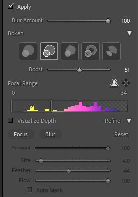
Its been an eye opener to go back through old 500mm f8 mirror lenses to find additional examples of how this now Blur Tool works. This, I used a Tamron 500mm mirror lens. I picked out this one as an example to show. I do think Adobe does have more work to do to improve the masking as it is far from perfect. I did have to manually edit this mask where mistakes had been made.
Image 1 is the Before
Image 2 is the After
Image 3 is the 3D Mask
Image 4 shows the key for the 3D mask where it color codes nearest to farthest. The box shown can be slid back and forth as needed, and it can be stretched as needed also to include a broader range of distances. Beneath it are a Focus and Blur option where a brush can be be used to manually fix the image.


Oct 22, 2023 20:45:59 #
Here is a summary of the expected number of Erase/Write cycles that can be expected from NAND Flash Memory from the Enterprise Storage Forum:
Please note that there are 3 cell type mentioned below: SLC, MLC and TLC
SLC = Single Level Cell. This the case that a cell has only two states -- zero or one. These are the early memory cards, and they were very rugged. But capacity and speed are low.
MLC = Multi Level Cell. This case allows each cell to store 2^2 states which is 4 levels. This means that the internal comparators have to be able to resolve Vdd/4 increments. If a part is working at 1.8V, then we would have 4 regions for the cell to output it's level. That would be 0 to < 0.45V, 0.45V to < 0.9V, 0.9V to < 1.35V, and 1.35V to 1.8V. This means that one cell contains 4 possible states and we could call them 00, 01, 10, and 11 -- two bits per cell.
TLC - Triple Level Cell and this time it is 2^3 = 8 states, meaning that it can store 000, 001, 010, 011, 100, 101, 110, 111 or 3 bits of data per cell.
To make this even more challenging, each generation becomes faster, and the data stored in each cell has to be 8 repeatable distributions as a shift in level would make it read a different group of 3 bits.
Note also that they mention the number of Write Cyles. Understand that in order to do a write cycle, a block needs to be erased first, thus Write Cycle = Erase Cycle / Write Cycle.
https://www.enterprisestorageforum.com/hardware/ssd-lifespan-how-long-will-your-ssd-work/
How SSD/Flash Endurance is Measured
The endurance rating of NAND flash SSDs is expressed in write cycles. They have a limited number of write cycles, after which the oxide layer of the flash memory cells starts degrading. This impacts the performance of the SSD.
The endurance rate is also called the program/erase cycle, or P/E cycle. When new data is stored in the SSD, an existing data block must be erased electrically. Unfortunately, a continuous P/E cycle deteriorates the oxide layer of the NAND flash memory cells. Thus, these cells eventually wear out, which affects their data-storing capacity.
Another undesirable phenomenon that affects SSD performance is write amplification. When writing data into the storage drive, the actual amount of the write gets multiplied. This increases the number of writes and thus shortens the reliable operation time of the SSD, crashing its consistency. Different factors affecting the write amplification are garbage collection, over-provisioning, metadata, log structures, and de-duplication.
You will find key differences in the flash endurance of single-level cell (SLC), multi-level cell (MLC), and triple-level cell (TLC) architecture:
SLC NAND flash can endure around 50,000 to 1,00,000 write cycles.
MLC NAND flash can sustain up to 3,000 write cycles. eMLC or enterprise MLC version supports about 10,000 write cycles.
TLC NAND Flash has low endurance and can take about 300 to 1,000 write cycles.
Note: There are others papers that specify different numbers max write cycles.